| | | | | | | | | | | |
| All rights reserved. |
| Step 6 |
Our basic explanation is split into several steps

Page 1
Page 2
More information on how it works

VPPEM can be used to give depth profiles.
This figure from Page 5 shows a VPPEM spectrum. The spectrum is
along the photon energy axis for a fixed detection energy of 1.0 eV.
This data is from an oxidized Al surface taken from a spectral image
series with photon energies from 72.5 eV to 85.0 eV in 0.5 eV steps.
The NEXAFS signal is at 74.5 eV, and the Al metal XPS signal is at the
work function plus the detected electron energy, 1.0 eV, higher in
energy. The detector window is 0.25 eV.
This spectrum was taken at one energy. That is to say we are
detecting only those electrons that have 1.0 eV kinetic energy when
leaving the surface.
We can change the detection energy by changing the bias on the
sample.
When we change the bias we see that the XPS peaks move to higher
energies, but the NEXAFS edge at 74.5 eV stays the same.

The spectra above make a two dimensional image data set for each
pixel: detection energy and photon energy.
The spectra are measured from 65.0 to 95.0 eV in steps of 1.0 eV, and
with detection energies 1.0, 2.0, 5.0, and 10 eV, a,b,c,d respectively.
The background levels have been suppressed to arrange the
individual spectra in the graph.
The spectra show that there is a 2p absorption edge in the region of
74.5 eV, and there are two Al 2p photo peaks, the peak originating in
the metal is indicated by the letter m, and in the oxide by the letter o.
As the detected energy is changed to a higher value (by reducing the
sample bias) the two Al 2p photo peaks, m and o, move together to
higher photon energy, and get relatively larger.
As the Al metal 2p photo peak moves higher in energy with a
higher detection energy, we find that a further feature appears
with a peak at 79.0 eV, just below the initial metal photo peak
position at 80.0 eV, and 4.0 eV above the 2p edge.
The binding energy of this new feature remains at 79.0 eV as we
increase the detection energy to 10.0 eV. There also appears to
be a third peak, 3.0 eV higher than the 79.0 eV peak, with the
same general characteristics. These two additional features can
be identified as Al 2p edges from amorphous aluminum oxide.
A clear feature of the spectral series is the change of relative
intensity between the Al metal, and oxide photo peaks with
detection energy.
This change in relative intensity gives us data for depth profiling
through changes in attenuation length with detection energy.
The 2p Al metal absorption edge defines the Fermi level energy for
binding energies above it. This gives us a direct measure of the
energy above the Fermi energy of the photo electrons in the aluminum.
From the spectral series above, we have the Al 2p metal photo peaks
(m) at 80.0, 81.0, 84.0, and 89.0 eV, then the energies in the
aluminum are 5.0, 6.0, 9.0, and 14.0 eV respectively.
If the Fermi energies of the oxide, and the metal are aligned, we can
expect the same energies in the oxide. The Al metal, and oxide
photoelectrons pass through the same surface potential barrier, with
the same final energy, and their energies in the oxide will be the same.
We can create a model of how the electrons escape into the vacuum
and estimate the oxide layer thickness.
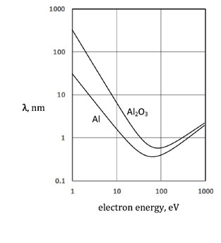
This graph shows that electron energies in the 5-15 eV range are
on the rapidly changing lower part of the curves. This makes relative
peak intensities very sensitive to changes in thickness in the metal
is 4.1 nm, and for 14.0 eV it is 1.7 nm. In the oxide, the mean free
paths are 22.2 nm and 4.8 nm respectively.
on the rapidly changing lower part of the curves. This makes relative
peak intensities very sensitive to changes in thickness in the metal
is 4.1 nm, and for 14.0 eV it is 1.7 nm. In the oxide, the mean free
paths are 22.2 nm and 4.8 nm respectively.
The experimental results are best fitted with oxide overlayer of 3.5 nm.
| | | | | | | |
| How it works |